Research

Tap a card to flip between the photo and the write-up. Scroll the text, then keep going for the next topic.

  1. 01 — Research stream

    Bridging Lab-Scale Optimization to Scalable Ambient Perovskite Manufacturing

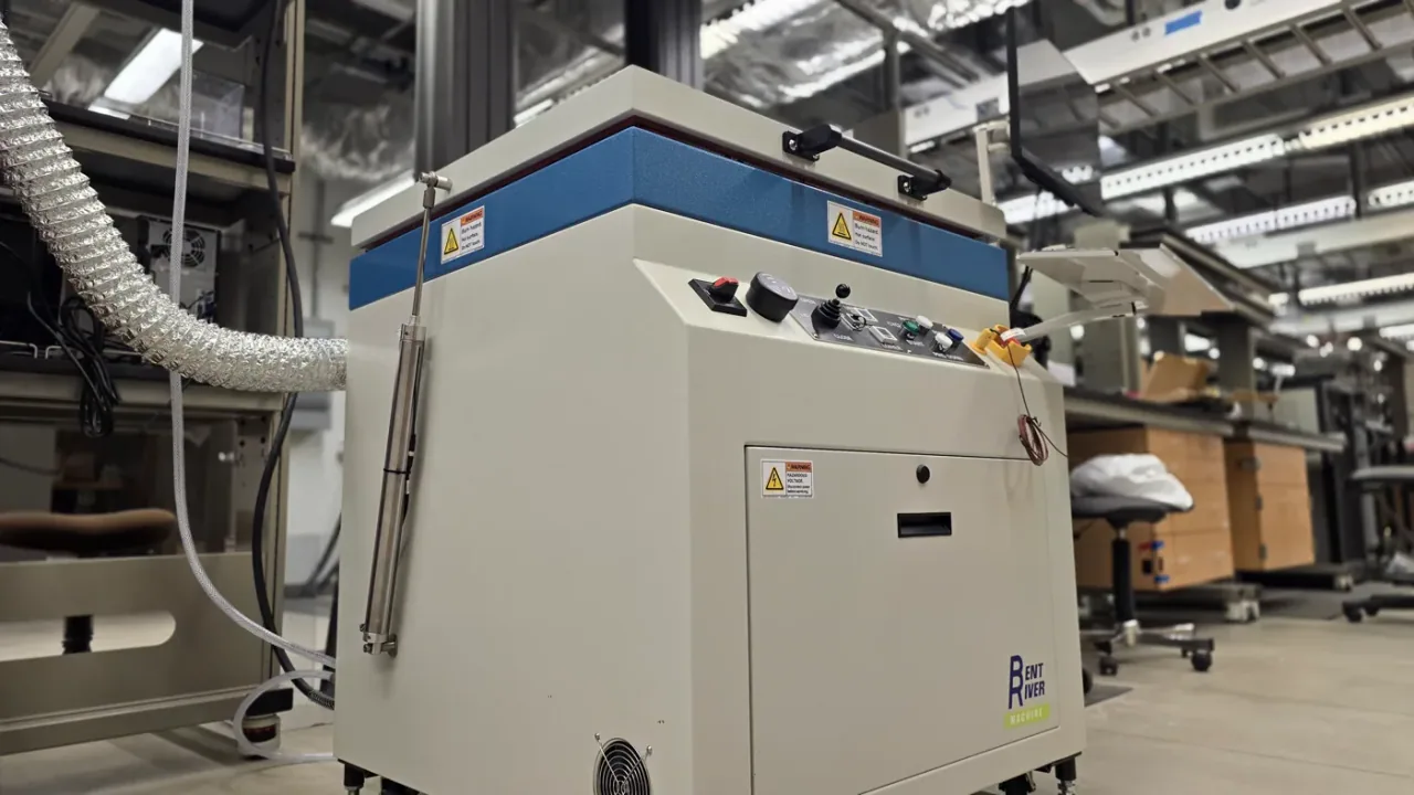
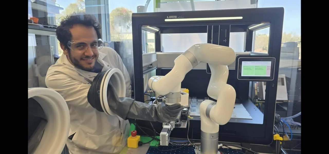
    We scale up our PASCAL (autonomous robot) small-area recipes into high-throughput, large-area coating protocols using the AutoVerde slot-die coater.

    By integrating automation with rapid process optimization, we enable a smooth transition from lab-scale discovery to ambient-compatible, scalable fabrication.

    This approach ensures uniform film deposition across large substrates and supports the development of reproducible and efficient perovskite devices.

    Our work brings a sense of momentum and creativity, driving innovation in scalable materials processing for next-generation photovoltaics.

  2. 02 — Research stream

    Ternary Phosphides for Solar

    In collaboration with groups around the country, the Fenning Research Group is at the forefront of studying ternary phosphides (AM2P2) for solar applications. Guided by state-of-the-art computational techniques, the AM2P2 materials have been identified as environmentally robust, defect tolerant, band-gap tunable photo-absorbers which are beginning to gain significant attention from the community.

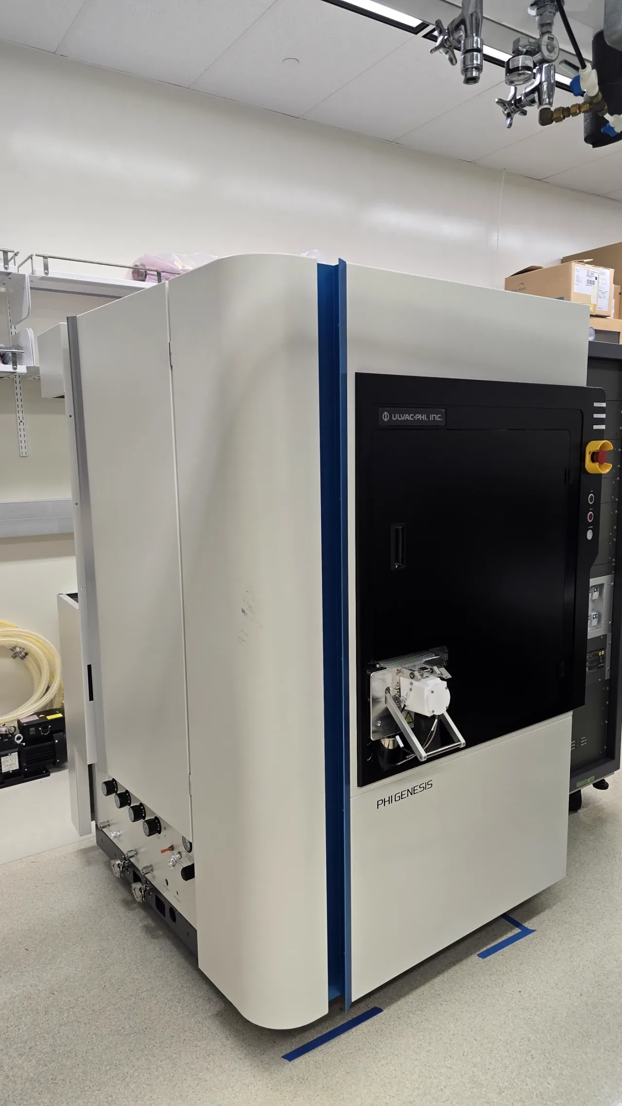
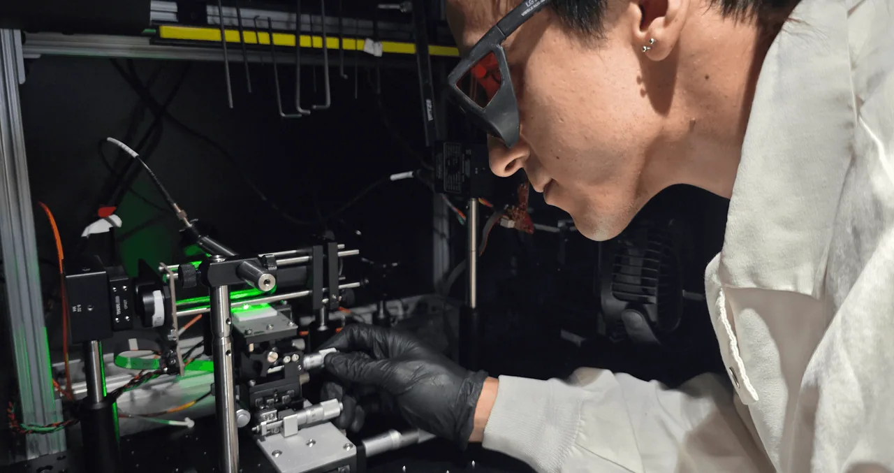
    Like with other semiconductors, the AM2P2 surfaces play an outsized role in the electronic performance of these materials, and within our group we aim to understand the phenomena in play at these interfaces. By making use of surface sensitive techniques, such as XPS, we can study their rich surface chemistry and can provide insights into the nature of the surface states. Techniques such as wavelength dependent μ-PL allow us to assess the quality of the surface passivation methods which will be key in further enhancing the optoelectronic performance of these materials.

    Lastly, we are very interested in the use of these materials for photo-electrochemical applications, where their exceptional stability can be leveraged in the production of solar fuels, especially when paired with co-catalysts.

    Future work aiming to optimize the performance of these absorbers, and their interplay with other materials, will likely benefit not just from perfectly tailoring their interfaces, but also better understanding and leveraging their innate self-passivating properties. Such insights could have potential impacts not just on these materials, but on semiconductors and solar absorbers as a whole, and we aim to pave the way in these pursuits.
  3. 03 — Research stream

    Module Design for Circularity & Recycling

    As solar PV scales globally, module waste is becoming a critical issue. To address this, the Fenning Research Group is advancing PV packaging designed for circularity.

  4. 04 — Research stream

    Catalysis

    Catalysis is the key to enabling greener chemical transformations (energy storage, fertilizer production, etc.) that powers our modern world. One of the biggest challenges in catalysis remains the breaking of linear scaling relationships.

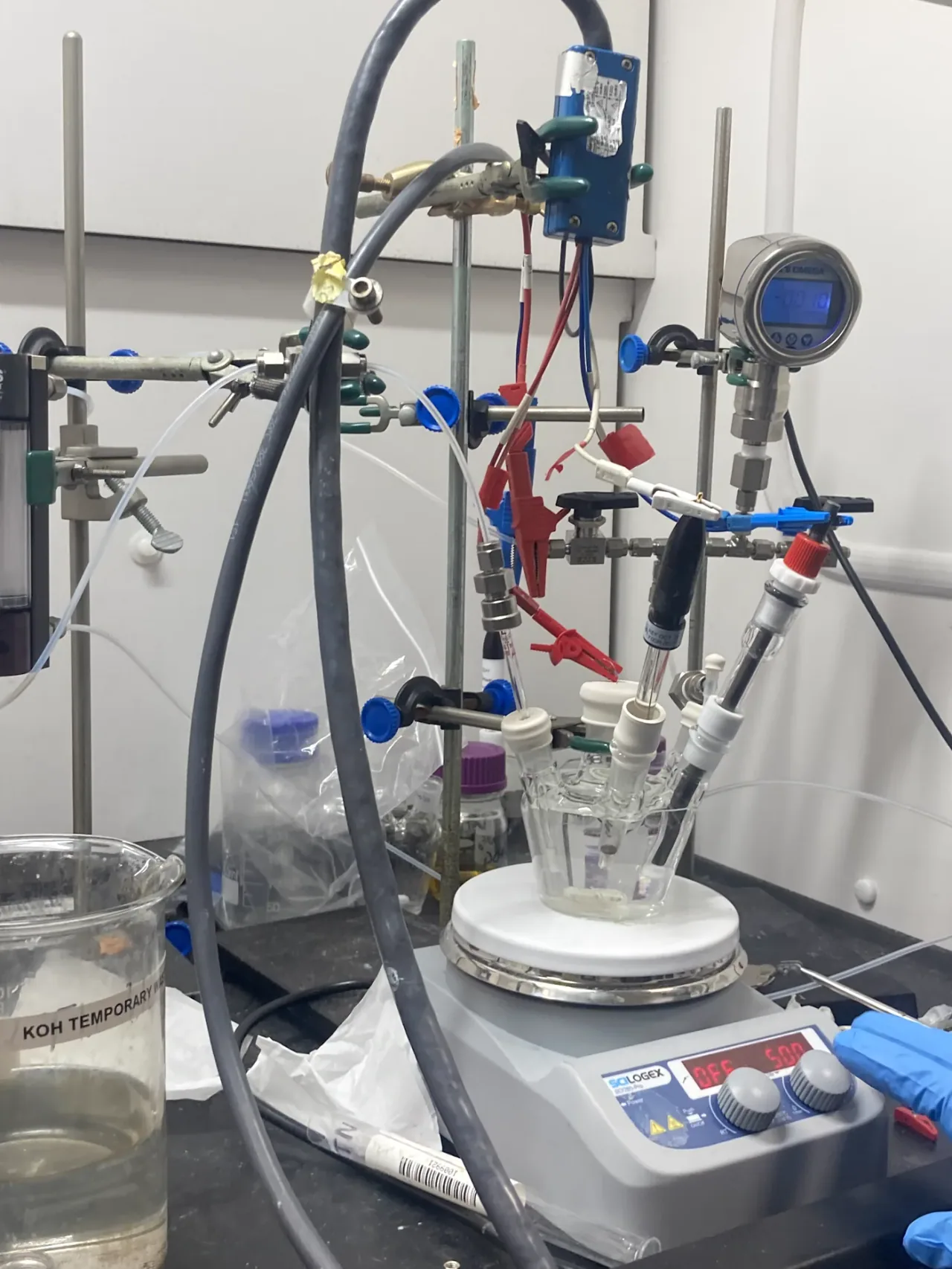
    Though many strategies have been tried and tested, none are as widely applicable as a catalyst with a switchable binding energy. Though much theoretical work has been done on these dynamic catalysts, experimental realizations remain scant. We aim to use ferroelectric perovskites as a platform to experimentally probe dynamic catalysis.

  5. 05 — Research stream

    Synchrotron Microscopy

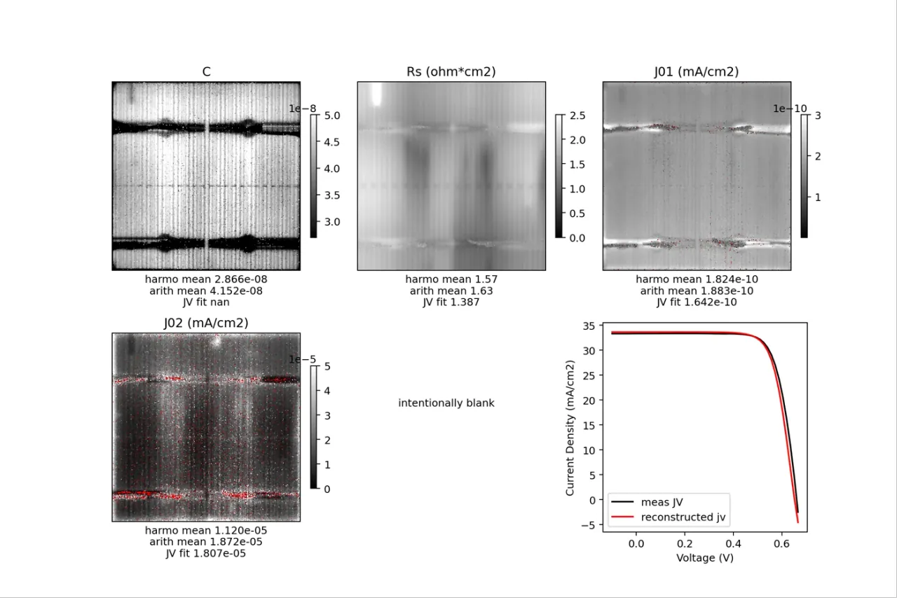
    One of our main research focuses is on advanced characterization of defects in photoactive materials. We use synchrotron-based X-ray microscopies to better understand the formation of nanoscopic defects in halide perovskites for photovoltaic applications. We perform measurements at several synchrotrons including the Advanced Photon Source at Argonne National Laboratory and the Advanced Light Source at Lawrence Berkeley National Laboratory.

    At the Advanced Photon Source, we use hard (7–30 keV) X-rays to measure the nanoscale structural, chemical, and optoelectronic properties of solar absorbers, yielding valuable insight into how performance-limiting defects form and can be mitigated. At beamline 26-ID-C, we determine where structural defects form and how they correlate with local chemical variations via nanoprobe X-ray diffraction and fluorescence. At beamline 2-ID-D, we perform microprobe X-ray fluorescence, X-ray excited optical luminescence, and X-ray beam induced current measurements to correlate local chemical variations with optoelectronic and solar cell device performance. At beamline 19-ID-E (the in-situ Nanoprobe, a feature beamline created during the APS-U upgrade), we will measure these properties at the nanoscale in-situ during annealing of the perovskite. This unprecedented capability, which we have worked hand-in-hand with beamline scientists to design and optimize for perovskite solar cells, will enable direct observation of nanoscopic defect formation in real time.

    At the Advanced Light Source, we measure crystallization of our perovskites in-situ during spin-coating and annealing using wide-angle X-ray scattering (WAXS) at beamline 12-3-2. Through these measurements, we can track the evolution of different phases to elucidate crystallization pathways. The understanding and control of these pathways is critical to determining the final state of the perovskite and its performance as a solar cell.