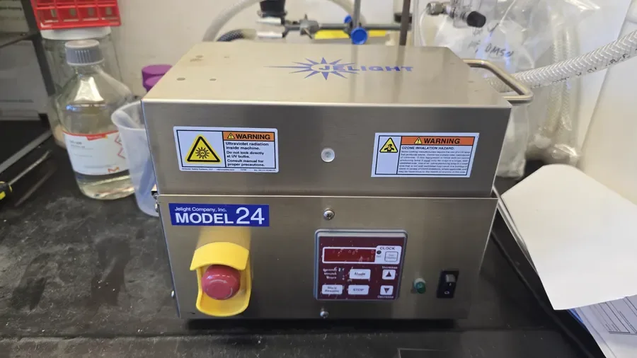
UV ozone treatment
Surface cleaning and preparation before thin-film deposition and device fabrication.
Navigation
From discovery to device
Our lab combines automated perovskite processing, thin-film fabrication, electrochemistry, and advanced materials characterization. The group also leverages UC San Diego's shared-use Materials Research Center and Nano3 cleanroom and characterization facilities.
Automated synthesis
The Perovskite Automated Spin Coat Assembly Line (PASCAL) supports reproducible, high-throughput exploration of small-area perovskite recipes. Promising processes can then move toward larger-area, ambient-compatible coating workflows with the group's AutoVerde slot-die platform.
In-lab capabilities
A representative look at the systems supporting photovoltaic, catalysis, and materials research in the group.
Surface cleaning and preparation before thin-film deposition and device fabrication.
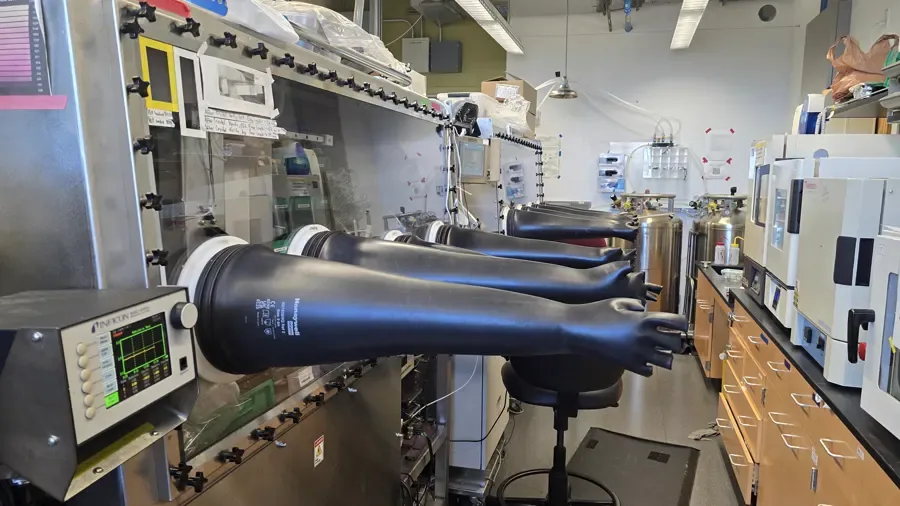
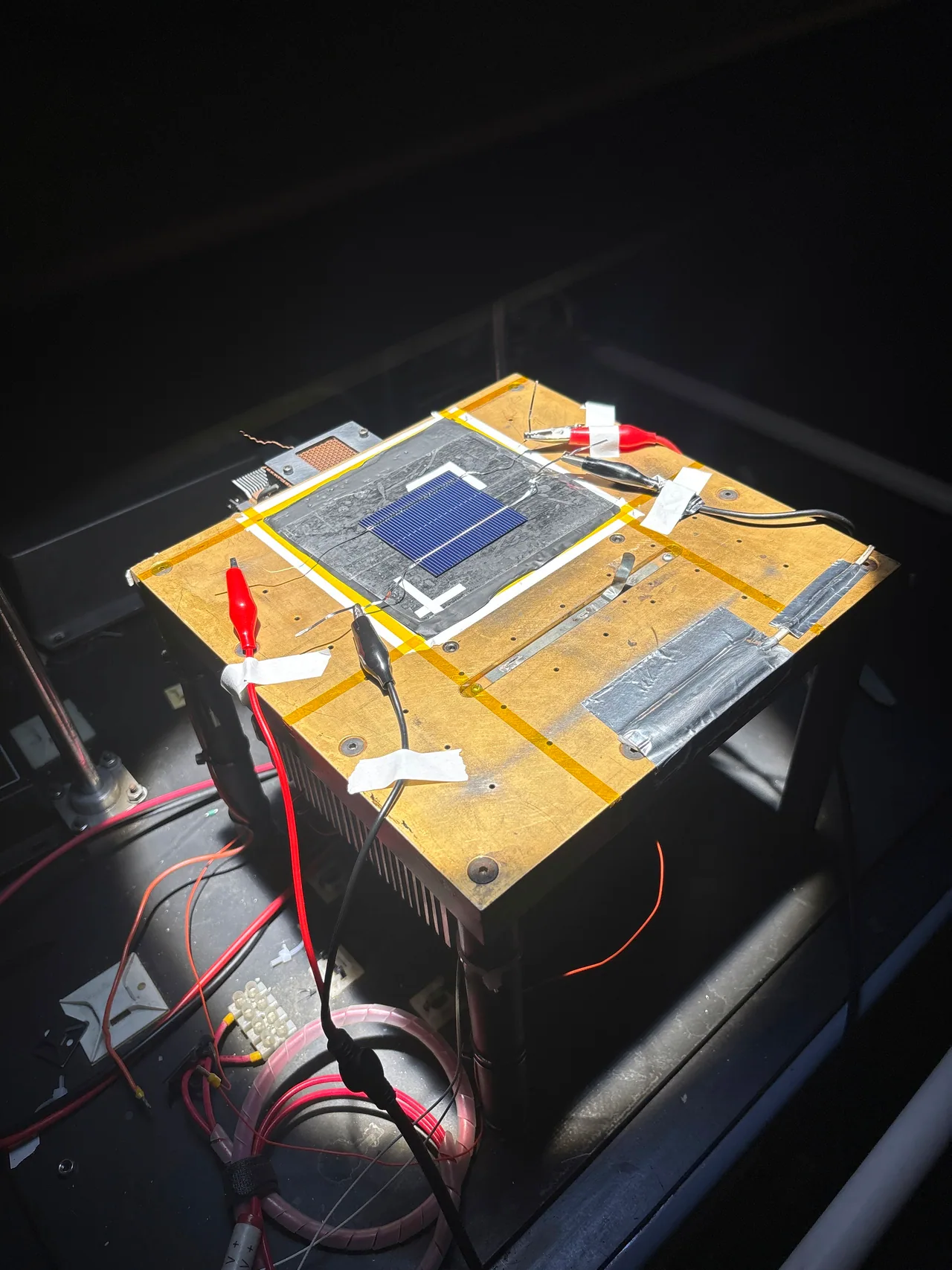
Controlled thin-film deposition for contacts, interfaces, and device stacks.
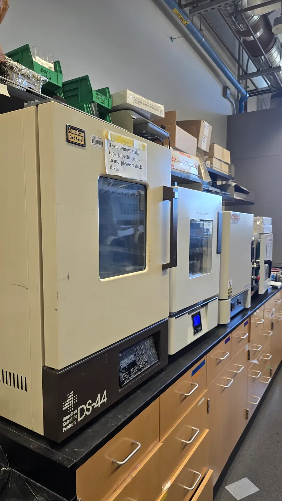
Dedicated ovens for controlled annealing and materials processing.
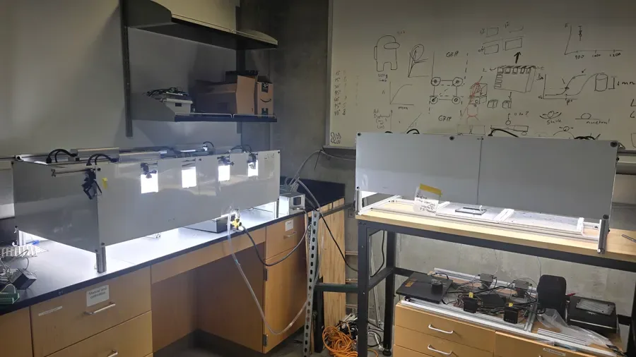
Environmental aging and stability studies for materials and photovoltaic devices.
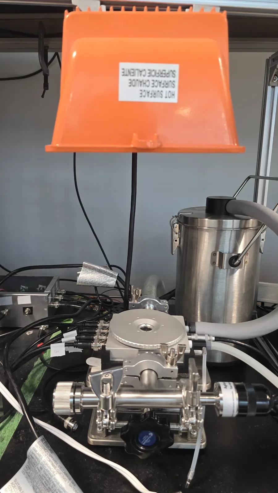
Temperature-dependent optical and electronic characterization.
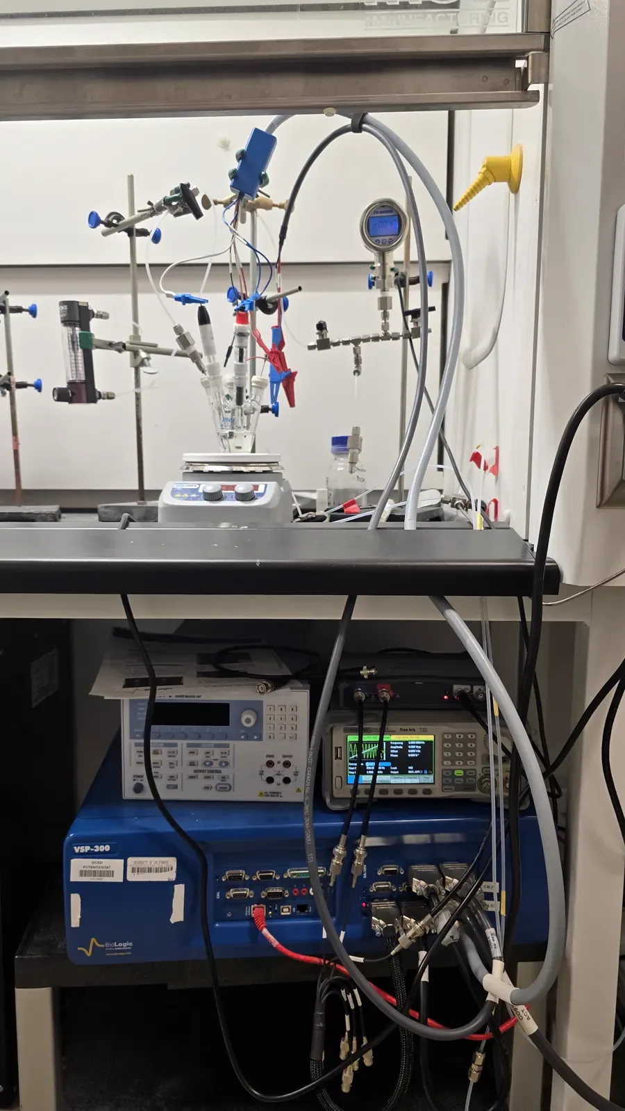
Electrochemical testing for catalysis, solar fuels, and interface studies.
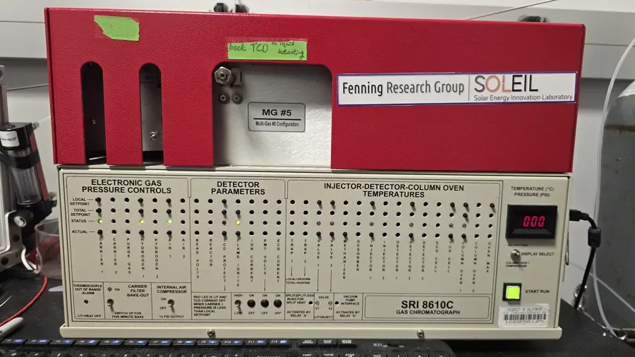
Product separation and analysis for catalytic reaction studies.
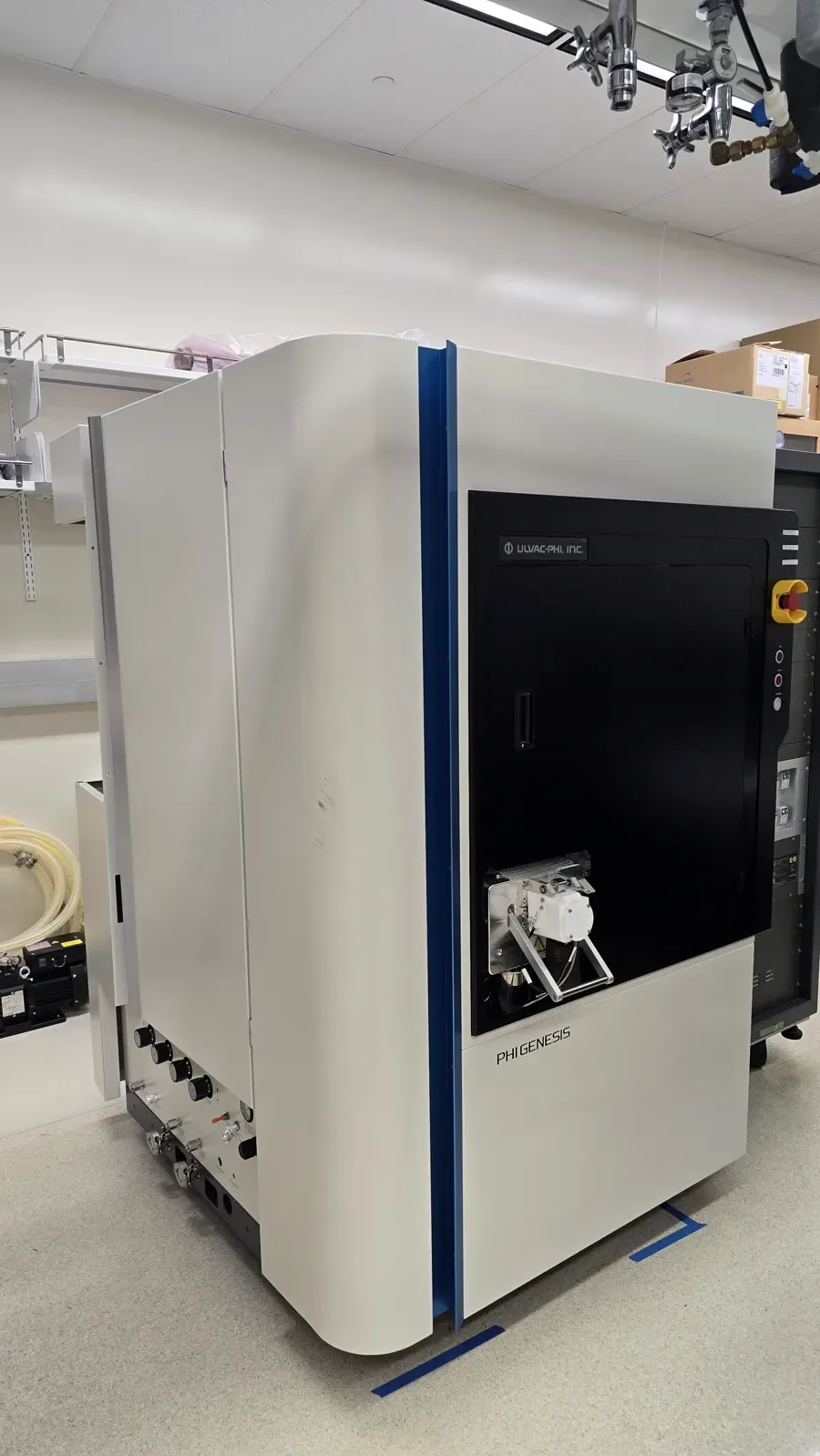
Surface-sensitive chemical and electronic-state analysis with the PHI Genesis XPS.
Shared UC San Diego infrastructure
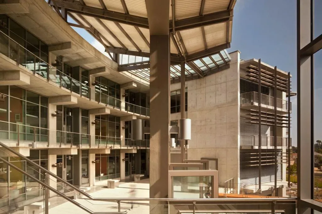 01
01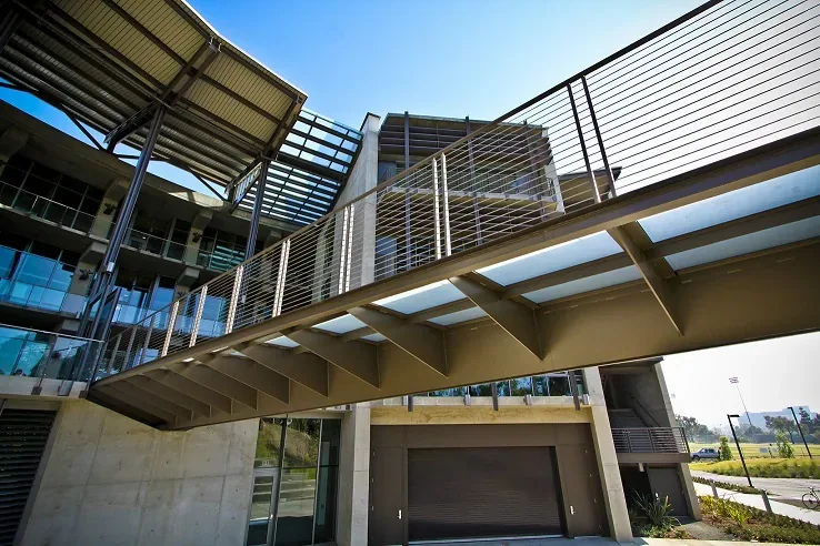
The 9,000-square-foot shared-use Materials Research Center occupies the basement of the Structural and Materials Engineering building. It gives the group walk-up access to diffraction, optical spectroscopy, and scanning-probe tools without leaving campus — the same instruments used across nanoengineering, chemistry, and materials science at UC San Diego.
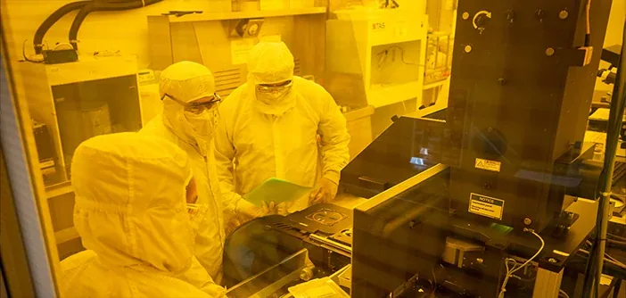 02
02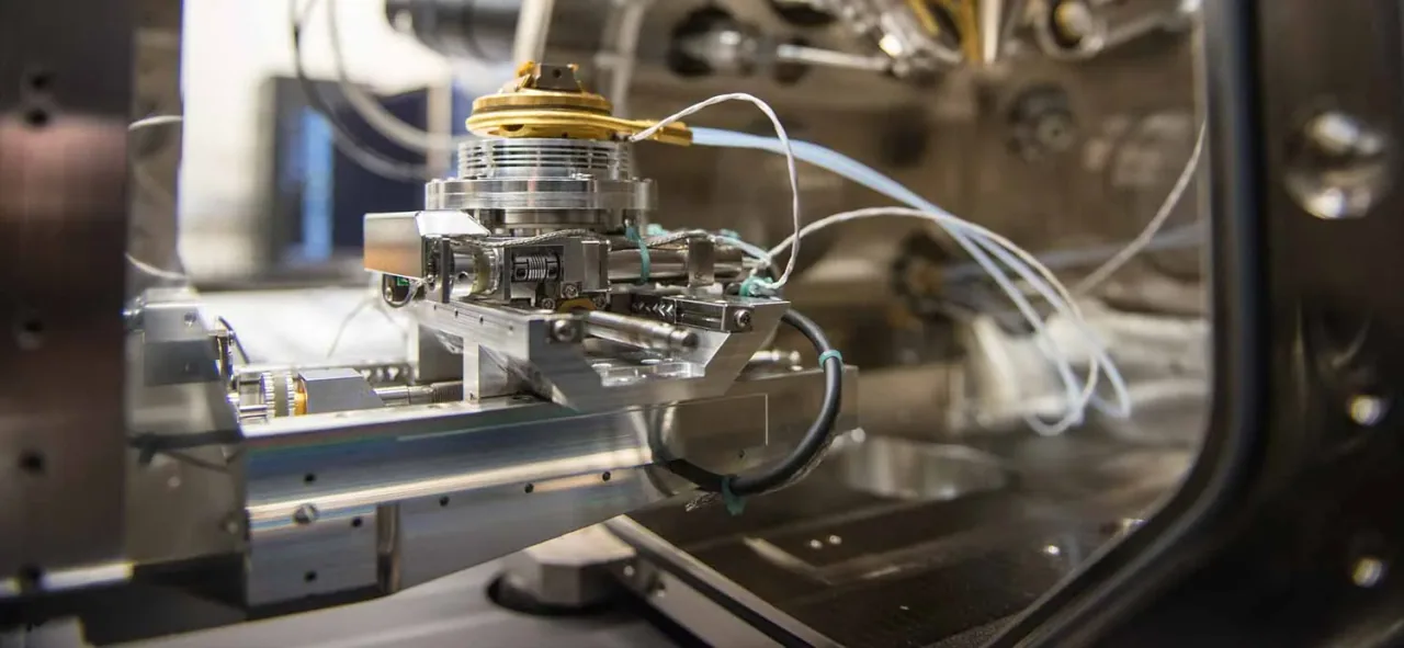
Nano3 is UC San Diego’s nanofabrication cleanroom in Atkinson Hall at the Qualcomm Institute — more than 7,000 square feet of Class 100 and Class 1000 space, plus a characterization suite used by hundreds of campus and industry groups. The Fenning group relies on it for lithography, thin-film deposition, and electron-beam imaging that go beyond what fits in a single lab.